>Stack#1 – Tube#1 – Thin dry oxide Tube#2 – Thin oxynitride Tube#3 – Anneal > Stack#2 – Tube#1 – Pyrogenic oxide Tube#2 – LTO Tube#3 – Silicon nitride >Stack#3 – Tube#1 – Drive-in Tube#2 – Intrinsic poly silicon Tube#3 – N-type doped poly silicon -6inch wafer, 50 wafers/batch (include dummy) -3-zone heater, max.1200? -Alumina twin […]
-
Mail ID : info@hcptech.in
-
CALL US : 080 6646 8218
Archive for May 28th, 2025

Single Wafer Cleaning, Resist Processing, and Wet Etching Technology
NANO-MASTER state-of-the-art Cleaning and Processing Technology incorporates patented damage free megasonic cleaning, chemical cleaning, brush cleaning, high pressure and drying in one process step. To achieve maximum cleaning optimization without substrate damage, the megasonic energy density must be kept slightly below the damage threshold at any point on the sample. NANO-MASTERs patented technology assures uniform […]
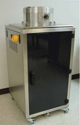
Thermal Vacuum Systems
Features: 36 Hr Auto Run with Preprogrammed Heating and Cooling Cycles Computer Controlled, Safety Interlocks Multiple Levels of Access with Passwords Chamber Size: 43 in Length and 24 in Diameter Sliding Thermal Platform of 16 x 32 Thermal Platform can be Heated to 150 °C and Cooled to -100 […]
Plasma Cleaning and Ashing Systems
NANO-MASTER Plasma Ashing and Cleaning Systems are designed to meet a wide range of needs from wafer resist stripping to surface modification of batch as single wafer loads. They are PC controlled systems with various plasma sources, heated and unheated substrate holders and unique ability to switch from plasma etch to RIE etch modes. Applications: […]
PECVD Systems
NANO-MASTER PECVD systems are capable of depositing high quality SiO2, Si3N4, or DLC films on up to 8 diameter substrate size. To generate plasma, it uses RF shower head electrode or hollow cathode RF plasma source with fractal gas distribution. The platen can be biased with RF or pulsed DC and it is heated resistively […]
Ion Beam Etching Systems
Etching of metals which do not have volatile compounds such as Cu and Au cannot be accomplished in RIE Systems; however, physical etching with accelerating Ar ions is possible. Typically, surface is patterned with thick resist for masking and the energetic ion flux during etching overheats the substrate and the resist. Unless efficient means of […]

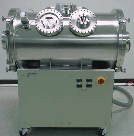
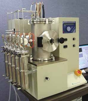
Reactive Ion Etching Systems
The NRE-4000 is a stand alone Reactive Ion Etching (RIE) System with shower head gas distribution and water cooled RF platen. It has a stainless steel cabinet and a 13 cylindrical Aluminum chamber that opens from top for wafer loading. Chamber has two ports, one with a 2 window and the other with a blank […]
Atomic Layer Deposition Systems
Atomic Layer Deposition is a thin film deposition technique that allows putting defect-free conformal layers of atoms. The process consists of sequential introduction of desired precursor vapors with hydroxyl groups, each of which forms about one atomic layer per pulse. Key challenges relate to fast removal of gas in the chamber to enhance throughput as […]
Plasma Assisted MOCVD Systems
NANO-MASTER has developed the first Table Top Plasma Assisted Metal Organic Chemical Vapor Deposition (PA-MOCVD) System for InGaN and AlGaN deposition processes. The features include five bubblers with individual cooling baths, heated gas lines, 950 °C platen, three gas rings, RF plasma source with shower head gas distribution and N2 flush at the end of […]