
-
Mail ID : info@hcptech.in
-
CALL US : 080 6646 8218
Blog


Wafer Bump 3D Vision Inspection
? Conduct with PASS Buffer when REWORK Part with Multiple NGs ? Function to start manufacturing with the REWORK Parts during INSPECTION ATM Check ? Apply the LOAD PORT substitute loading system during UNLOADER PART ATM inspection ? AIR CHUCK Works on Both 8-inch(200mm), 12inch(300mm) WAFER ? Users can output and monitor the designated DATA […]

3D Wafer Bump & Wire Bonding AOI Inspection system
ZEUS: 3D Wafer Bump & Wire Bonding AOI Inspection system ? Highest quality 3D Wire-Inspection. ? With high-resolution, complete inspection is possible even for Foot-shape. ? Inspect Mirror-surface without Reflection problem. ? As for PEMTRON’S unique optical technology, Coaxial lighting was applied to 3D installation. ? All Packages including SIP / FCBGA / FOWLP / […]
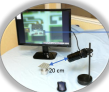
Inspection Camera
Visual inspection of micro assembly, Optical Zooming capability x 10, FOV 2mm up to 20mm Camera Ultra HD 5Mpx NumericZoom x 11 Combinedinspection of bonds & placements 20 cm sharpness and precision PC + Screen 22 Image capture/movie record Vision of picking, operations and place Tilt […]
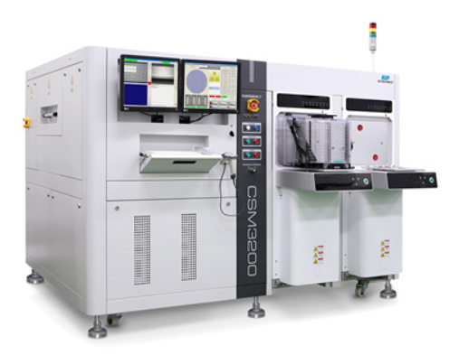
Laser Wafer Marker
CSM series is the wafer level chip scale marker for semiconductor and can mark on wafer backside without any chip damages.The equipment has an automated calibration system to compensate scanner accuracy and an automated marking inspection system to check the marking results.

Semiconductor Grinding Machine
The JL-D16 is primarily utilized for double-sided grinding or polishing of flat workpieces. It can also be employed for processing workpiece thicknesses, with a minimum achievable thickness of 0.4mm. Additionally, the surface precision can reach 0.3?m, ensuring a high level of machining accuracy. The innovative JL-D16 double-sided grinding machine combines both double-sided grinding and polishing […]

Lapping and Polishing machines
Hydrodynamic plain bearing:standard equipment for every model (Patented by HAMAI) Levitates the lower plate with the hydraulic force, thereby ensuring highly load-resistant, smooth, and vibration-free rotation of the plate. Plate flatness maintenance cycle:standard equipment for most of the machines. Rotates the carriers clockwise and counterclockwise alternately to maintain the flatness of the plate surface while […]
Laser Tray Marker
Tray marker for semiconductor can be manufactured as compact U type and conventional “I” type.

Laser Strip Marker
The 4-beam strip marker for semiconductor can support both slot and stack magazine for loading & unloading. The strip handling is divided into two types, shuttle and rail types and the loading/unloading methods such as 1 in 1 out, 2 in 2 out and etc. can be configured in accordance with customers’ request.

Laser Drilling
BMC204P is a package drilling equipment for the strip and wafer types of POP.Its automatic inspection and scanner compensation feature make the process highly accurate.It adopts flying processing method to increase productivity.

Laser Dicing
LMC3200D is a dicing system for thin wafer of less than 200?.It is better than mechanical blade dicing system in terms of COO, sicne it doesnt need to replace blade and the lifetime of laser parts is long and semipermanent.The non-contact process can dramatically reduce the problem of chipping and enable high-speed processing.