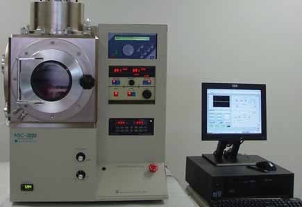
NANO-MASTER Plasma Ashing and Cleaning Systems are designed to meet a wide range of needs from wafer resist stripping to surface modification of batch as single wafer loads. They are PC controlled systems with various plasma sources, heated and unheated substrate holders and unique ability to switch from plasma etch to RIE etch modes.
Applications:
Removal of Organic and Inorganic Materials without Residues
Photoresist Stripping or Ashing
Desmearing and Etch Back Applications
Cleaning Microelectronics, Drilled Holes on Circuit Boards or Cu Lead Frames
Adhesion Promotion, Elimination of Bonding Problems
Surface Modification of Plastics: O2 Treatment for Paintability
Producing Hydrophilic or Hydrophobic Surfaces
Leave A Comment