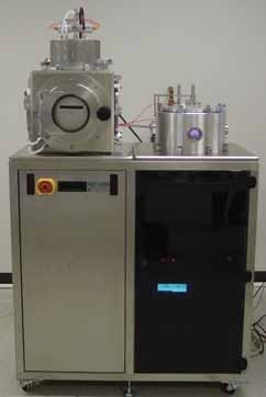
NANO-MASTER PECVD systems are capable of depositing high quality SiO2, Si3N4, or DLC films on up to 8 diameter substrate size. To generate plasma, it uses RF shower head electrode or hollow cathode RF plasma source with fractal gas distribution. The platen can be biased with RF or pulsed DC and it is heated resistively […]
-
Mail ID : info@hcptech.in
-
CALL US : 080 6646 8218
Semicon Front End Manufacturing Tools
Plasma Cleaning and Ashing Systems
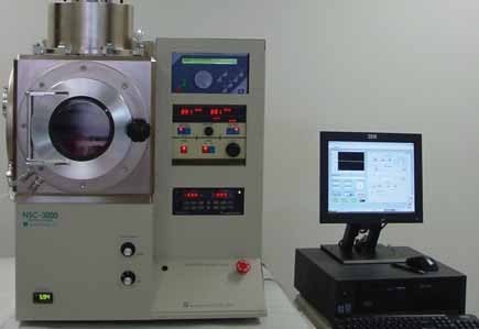
NANO-MASTER Plasma Ashing and Cleaning Systems are designed to meet a wide range of needs from wafer resist stripping to surface modification of batch as single wafer loads. They are PC controlled systems with various plasma sources, heated and unheated substrate holders and unique ability to switch from plasma etch to RIE etch modes. Applications: […]
Atmospheric Pressure Sputtering
AURION offers custom made sputtering systems in divers configurations. There are small lab systems with single circular cathodes, batch type systems with rectangular cathodes as well as inline machines
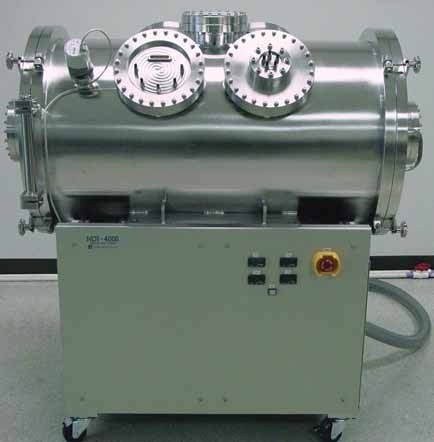
Thermal Vacuum Systems
Features: 36 Hr Auto Run with Preprogrammed Heating and Cooling Cycles Computer Controlled, Safety Interlocks Multiple Levels of Access with Passwords Chamber Size: 43 in Length and 24 in Diameter Sliding Thermal Platform of 16 x 32 Thermal Platform can be Heated to 150 °C and Cooled to -100 […]
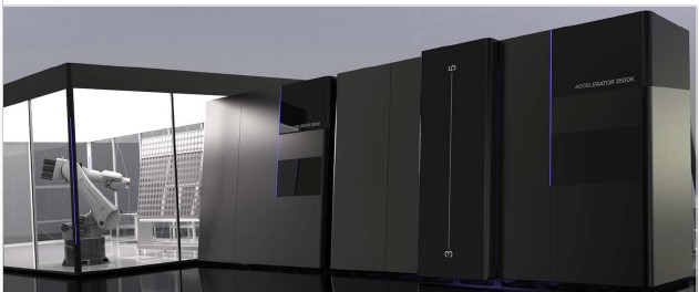
Epitaxy System – ENABLER 150K
The ENABLER 150K is a revolutionary system for the production of monocrystalline bulk acoustic wave filters. For modern and future generations of mobile communications, polycrystalline materials are no longer sufficient to accommodate higher frequencies. The new epitaxy approach of ELEMENT 35 ensures a much more efficient production of future filter elements for telecommunications with numerous […]

Single Wafer Cleaning, Resist Processing, and Wet Etching Technology
NANO-MASTER state-of-the-art Cleaning and Processing Technology incorporates patented damage free megasonic cleaning, chemical cleaning, brush cleaning, high pressure and drying in one process step. To achieve maximum cleaning optimization without substrate damage, the megasonic energy density must be kept slightly below the damage threshold at any point on the sample. NANO-MASTERs patented technology assures uniform […]
Horizontal LPCVD/Furnace System
>Stack#1 – Tube#1 – Thin dry oxide Tube#2 – Thin oxynitride Tube#3 – Anneal > Stack#2 – Tube#1 – Pyrogenic oxide Tube#2 – LTO Tube#3 – Silicon nitride >Stack#3 – Tube#1 – Drive-in Tube#2 – Intrinsic poly silicon Tube#3 – N-type doped poly silicon -6inch wafer, 50 wafers/batch (include dummy) -3-zone heater, max.1200? -Alumina twin […]